PCB Stack-Up Design Services
Optimize your multilayer PCB with professional stack-up planning for signal integrity and absolute reliability.
Request a Fast QuoteWhat is PCB Stack-Up?
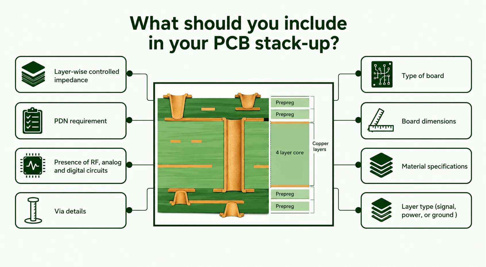
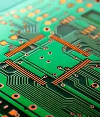
A PCB stack-up defines the strategic arrangement of copper and insulating dielectric layers in a printed circuit board prior to layout design. A highly optimized stack-up drastically reduces electromagnetic interference (EMI), enhances high-speed signal quality, and ensures seamless manufacturability. We offer tailored stack-up solutions spanning from simple 2-layer designs to highly complex 16+ layer High-Density Interconnect (HDI) PCBs.
Types of PCB Stack-Ups
Single Layer
Basic printed circuit board utilizing a single conductive copper layer.
Double Layer
Two copper layers supporting through-hole and SMT components for moderate complexity designs.
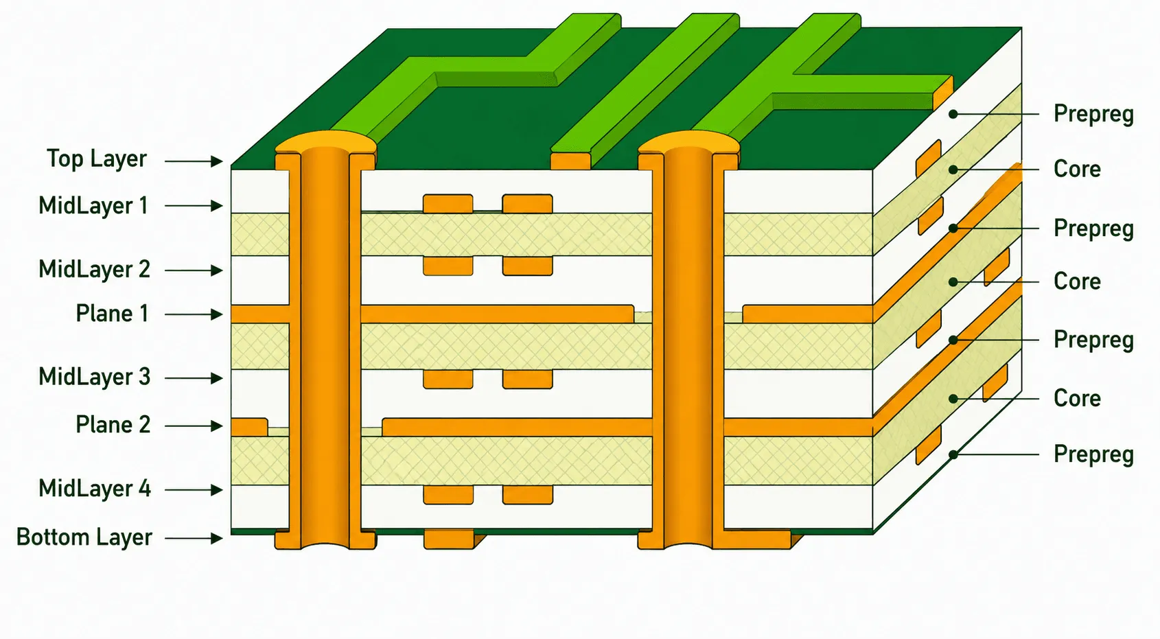
4-Layer
Dedicated signal, ground, and power planes ensuring highly stable and reliable designs.
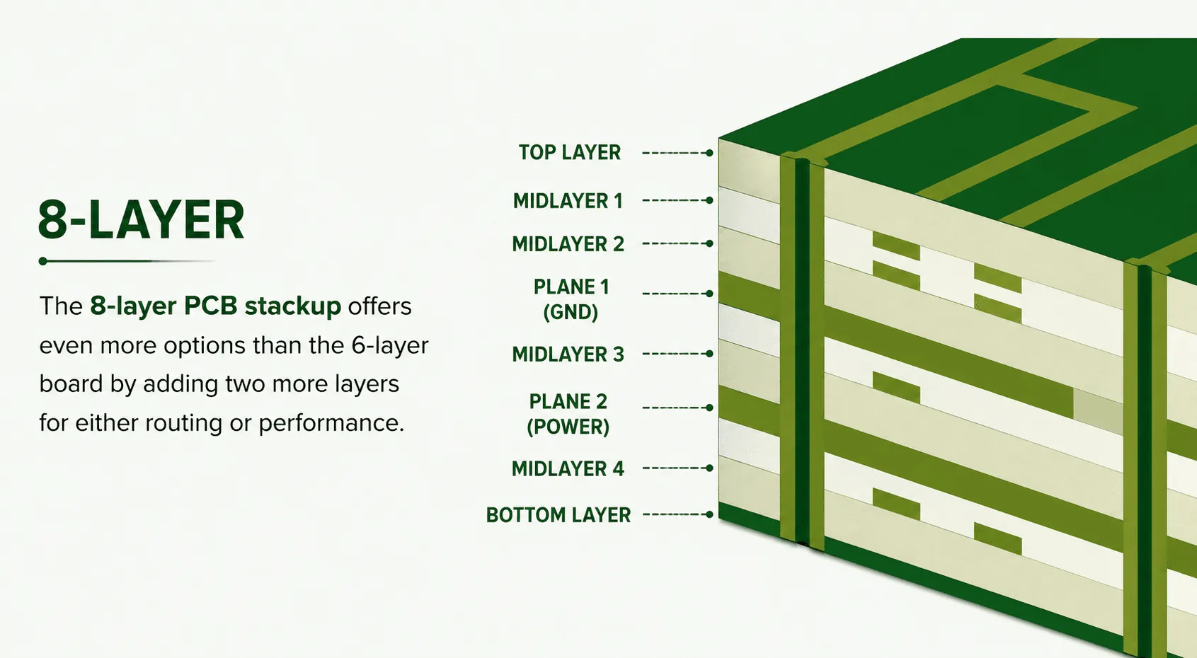
6-Layer & 8-Layer
Advanced configurations designed specifically for high-speed signals with multiple reference planes.
Typical Layer Stack Example (4-Layer)
| Layer | Material / Description |
|---|---|
| Top Layer | Copper + Soldermask + Silkscreen |
| Prepreg | Insulation layer (Dielectric) |
| Inner Layer 1 | Ground Plane (GND) |
| Core | Rigid Dielectric material (FR4) |
| Inner Layer 2 | Power Plane (VCC) |
| Prepreg | Insulation layer (Dielectric) |
| Bottom Layer | Copper + Soldermask + Silkscreen |
Applications & Industries
Telecom & Networking
Automotive Electronics
Medical Devices
Aerospace & Defense
Advantages of Proper Stack-Up Planning
- Improved signal integrity and significantly reduced routing crosstalk.
- Tightly controlled impedance matching critical for high-speed digital signals.
- Superior EMI/EMC compliance and overall noise reduction.
- Highly efficient thermal management and heat dissipation.
- Optimized for flawless PCB assembly processes.
Our Stack-Up Design Process
Requirement Analysis
Analyzing schematics and material limits.
Layer Planning
Structuring core, prepreg, and copper weight.
Simulation & Validation
Testing for target impedance and integrity.
Final Documentation
Exporting detailed stack-up charts for fabrication.
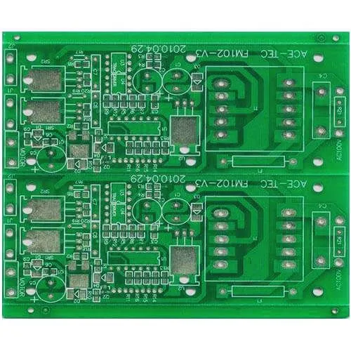
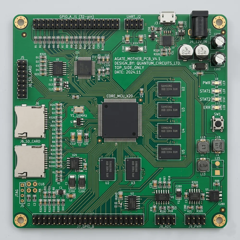
Sample Stack-Up Diagrams