Premium PCB Layout & Design for Prototypes to Mass‑Production
We turn schematics into manufacturable boards with controlled impedance, clean return paths, stack‑up planning, and assembly‑ready outputs (Gerbers, ODB++, pick‑and‑place, BOM).

Why Choose Us
Engineering‑first approach with strong DFM/DFT focus and EMI/EMC best practices.
High‑Speed Expertise
DDR, PCIe, MIPI, USB 3.x with skew/length matching and impedance control.
RF / Microwave
Stack‑ups for low‑loss materials, controlled transitions, and shielding strategy.
Manufacturable
IPC‑7351 footprints, Fab notes, panelization, and assembly‑ready outputs.
Quality & Review
ERC/DRC, checklist‑based peer reviews, and free DFM report with every job.
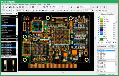
PCB Design Services
End‑to‑end from schematic capture to assembly files.
PCB Layout
2–20+ layers, analog, digital, mixed‑signal with proper PDN & return paths.
- Length matching & diff‑pair tuning
- Impedance controlled routing
- Thermal relief & copper balance
High‑Speed Design
DDRx, PCIe, Ethernet, HDMI, MIPI with constraints and timing closure.
- Skew budgeting & xTalk control
- Via strategy & back‑drilling
- Stack‑up co‑design with fab
RF & Microwave
50/75Ω lines, microstrip/stripline, controlled transitions & grounding.
- EMI/EMC best practices
- Shielding & keep‑out strategy
- Connector launch tuning
Flex / Rigid‑Flex
Bend radius rules, stiffener planning, and dynamic‑flex reliability.
- Coverlay openings & teardrops
- Hatched copper & strain relief
- ZIF/connector footprints
DFM/DFT Review
Fabrication constraints, assembly checks, test‑point planning & panelization.
- Solderability & tombstoning checks
- Pick‑and‑place verification
- AOI/ICT readiness
Deliverables
Complete outputs for fab & assembly.
- Gerber/ODB++, drill, fab notes
- BOM with MPN & alternates
- Pick‑and‑place, centroid, PDFs
Design Capabilities
We engineer for signal integrity, power integrity, and reliability.
- Up to 24 layers, blind/buried vias, via‑in‑pad, microvias
- Impedance control & stack‑up co‑design with fabricator
- PDN design with stitching vias & decoupling strategy
- Thermal analysis & copper balancing
- Compliance oriented (IPC‑2221/7351, RoHS/REACH)
- Libraries with 3D models & courtyard checks
How It Works
Transparent steps from requirement to release.
1. Requirement & NDA
Share schematics, constraints, preferred stack‑up, part libraries, and timelines. We can sign an NDA.
2. Feasibility & Quote
We assess complexity, propose milestones, and share a fixed quote or hourly estimate.
3. Layout Execution
Constraint‑driven routing with periodic design reviews and build‑ready checks.
4. Release & Support
Deliverables: Gerber/ODB++, drill, fab notes, panel, BOM, CPL. Free support until first proto spin.
What We Need for Quoting
- Schematics (PDF/Source) and block diagram
- Target board size, layers, interfaces, key ICs
- Speed classes (e.g., DDR3/4, PCIe Gen, USB 3.x)
- Specials: impedance, RF, flex, via‑in‑pad, microvia
- Any preferred standards, fab/assembly house
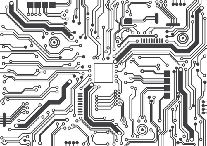
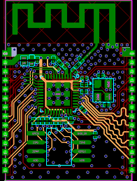
Recent Work
Representative renders and board photos (placeholders).
FAQ
Answers to common questions.
Ready to start your PCB design?
Share your schematics and constraints—we’ll revert with a plan and quote.
Start Now