PCB Stack-Up Design Services
Optimize your multilayer PCB with professional stack-up planning for signal integrity and reliability.
Request a Fast QuoteWhat is PCB Stack-Up?
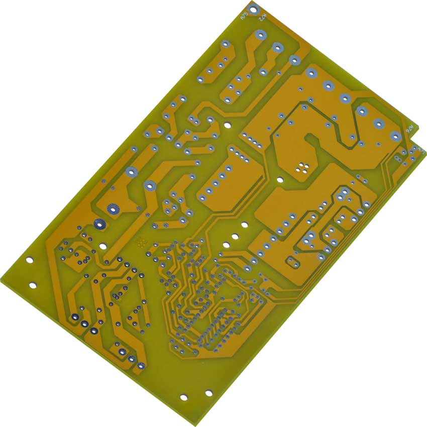
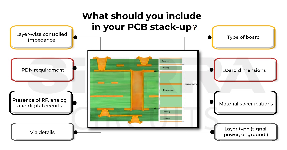
A PCB stack-up defines the arrangement of copper and insulating layers in a printed circuit board. A good stack-up reduces electromagnetic interference, enhances signal quality, and ensures manufacturability. We offer optimized stack-up solutions for simple 2-layer to complex 16+ layer PCBs.
Types of Stack-Ups
Single Layer
Basic PCB with one copper layer.
Double Layer
Two copper layers for moderate complexity designs.
4-Layer
Signal, ground, and power planes for stable designs.
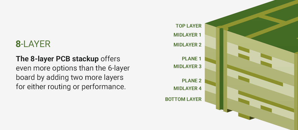
6-Layer & 8-Layer
For high-speed designs with multiple reference planes.
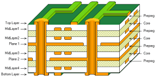
Typical Layer Stack Example (4-Layer)
| Layer | Description |
|---|---|
| Top Layer | Copper + Soldermask + Silkscreen |
| Prepreg | Insulation layer |
| Inner Layer 1 | Ground Plane |
| Core | Dielectric material |
| Inner Layer 2 | Power Plane |
| Prepreg | Insulation layer |
| Bottom Layer | Copper + Soldermask + Silkscreen |
Applications & Industries
Telecom & Networking
Automotive Electronics
Medical Devices
Aerospace & Defense
Advantages of Proper Stack-Up
- Improved signal integrity and reduced crosstalk
- Controlled impedance for high-speed signals
- Better EMI/EMC performance
- Efficient thermal management
- Optimized manufacturability
Our Stack-Up Process
Requirement Analysis
Layer Planning
Simulation & Validation
Final Documentation
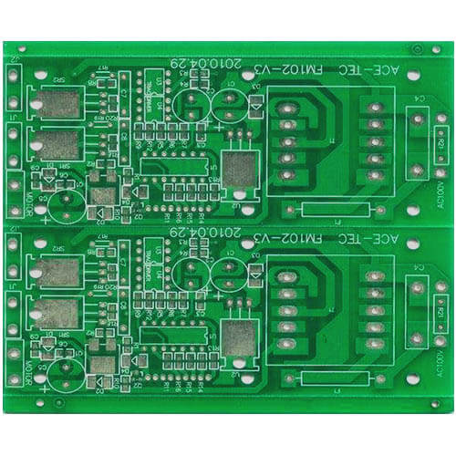
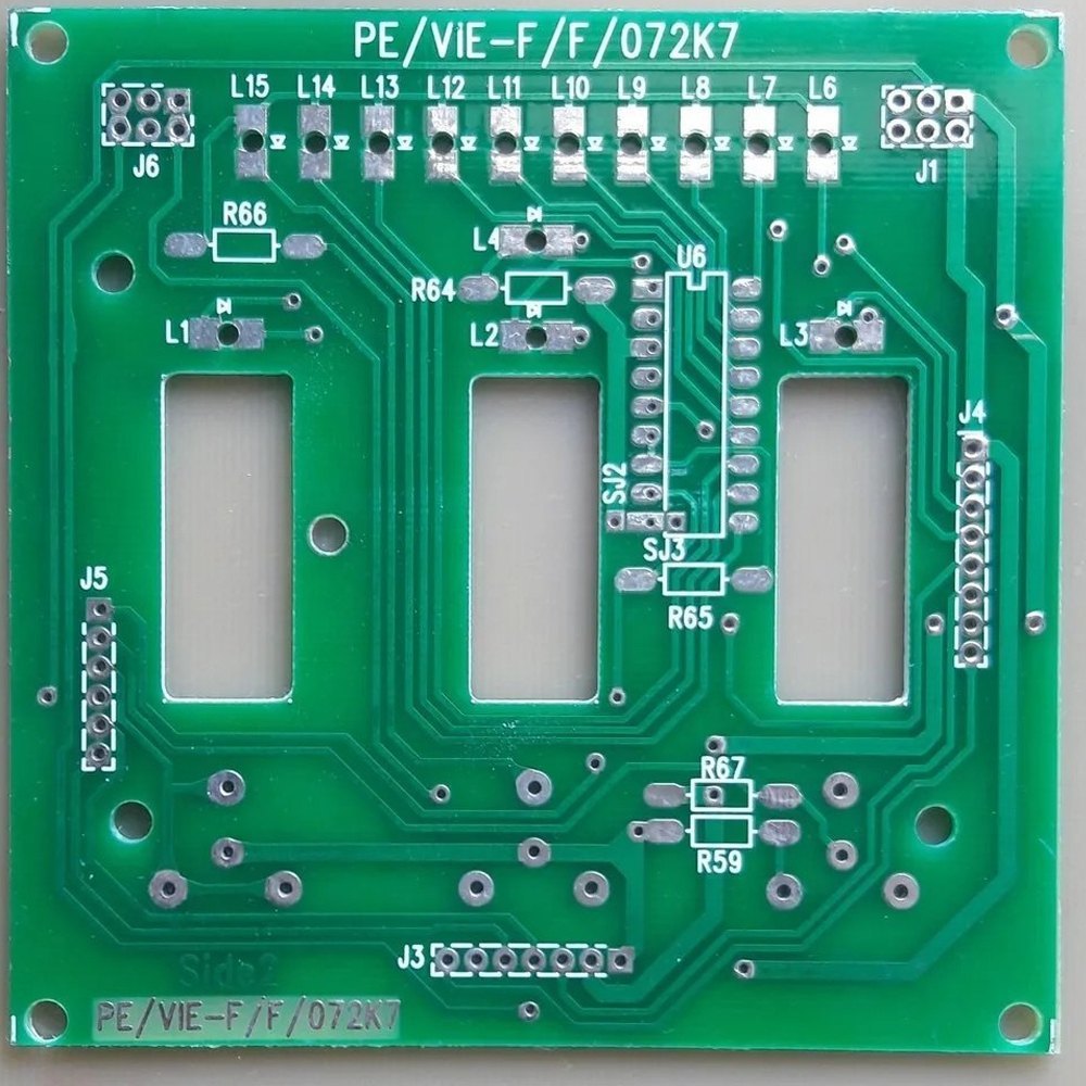
Sample Stack-Ups
Frequently Asked Questions
It improves signal quality, reduces EMI, and ensures reliable performance.
We support from 2 layers up to 16+ layers including HDI and RF boards.